
Europe Invests in Photonic Chips to Transform Chip Manufacturing
Europe is investing significantly in photonic chip technology, aiming to transform the semiconductor landscape and become a leader in this innovative field by 2030.
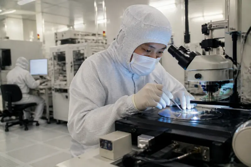
Europe is poised for a technological breakthrough in the computer chip industry with plans to develop photonic chips, which utilize light instead of electricity to process data. This initiative, backed by significant financial investments from the European Union and the Dutch government, aims to position Europe as a global leader in photonic technology.
What Are Photonic Chips?
Photonic chips represent a new frontier in chip manufacturing technology. Unlike traditional electronic chips that rely on electrical signals and can include billions of transistors, photonic chips utilize light, offering advantages such as faster data processing speeds, reduced energy consumption, and lower heat generation. Ton van Mol, a researcher at the Dutch research institute TNO, compared the current state of photonic technology to the early stages of electronic chips, emphasizing that the potential for growth and innovation is significant. Van Mol stated, "With optical chips, you are now where electronic chips were maybe 40 [or] 50 years ago." This comparison highlights the nascent stage of development for photonics, suggesting the technology is on the verge of significant advancements.
Investment and Support for Development
To bolster the development of photonic chips, the European Union has pledged €400 million (approximately $450 million; £330 million) towards a project named PIX Europe. This initiative aims to facilitate the creation of manufacturing facilities capable of producing integrated photonic circuits. The goal is clear: to remove reliance on US and Chinese chip manufacturers and foster a European manufacturing ecosystem. Van Mol explained, "We cannot depend like in the past that everything is manufactured in the US or China - that's not wise." The PIX Europe project is part of the broader European Chips Act, which focuses on enhancing local manufacturing capabilities. This strategic move is not only about self-sufficiency; it's about establishing Europe as a key player in the semiconductor industry.
Next Steps in Photonic Chip Development
Current manufacturing processes for photonic chips commonly use 4-inch (10 cm) wafers, but plans are underway to scale production to 6-inch wafers. TNO's facility, set to be operational by 2030, will specifically focus on producing six-inch indium phosphide wafers. This transition is significant as it will allow for the efficient production of larger chip quantities, crucial for meeting increasing global demand.
Collaboration with ASML
The success of photonic chip production is closely linked to the capabilities of ASML, a leading Dutch technology company renowned for manufacturing advanced semiconductor equipment. As van Mol indicated, the production methodologies of photonic chips are very similar to those of traditional electronic chips, requiring high-end clean rooms and similar wafer-based production processes. The collaboration is strategic, given that ASML's headquarters is located adjacent to the Eindhoven project site. Stanislas Baron from ASML highlighted that Europe possesses strong photonics research capabilities, stating, "The next challenge is translating those innovations into industrial-scale manufacturing." This cooperation aims to leverage advanced equipment and expertise in moving photonics from the research phase into large-scale manufacturing.
The Role of the Eindhoven Project
The new pilot production line at the High Tech Campus in Eindhoven has garnered support from influential figures such as Peter Wennink, former CEO of ASML. He described the project as "a launchpad for Europe's future digital economy." This facility is intended to serve multiple businesses, allowing them to design and manufacture chips without needing to invest in their own expensive production lines—a model similar to that of Taiwan’s TSMC, which is known for its dominant position in microchip manufacturing. The vision is to create a foundry model that attracts various companies to explore photonic chip capabilities and innovations at scale. Van Mol emphasized that the facility would operate on an order basis, producing chips customized to client specifications rather than focusing on any proprietary projects.

Market Outlook and International Competition
As Europe advances its photonic chip initiatives, the competitive landscape is becoming increasingly fierce. In June 2026, US-based Coherent announced plans for the world's first and largest volume-production six-inch indium phosphide manufacturing platform in Texas, supported by Nvidia and public funds under the US Chips Act. This highlights the global race to capitalize on photonic technologies and secure influential positions within the semiconductor sector, especially as AI and data processing demands continue to grow. As Joris Teer, a policy analyst at the European Institute for Security Studies, noted, "To retain influence, ensuring dependence on European parties rather than European autonomy is key." Teer’s comments reflect a recognition that Europe's re-industrialization strategy must focus on innovation in specific sectors, like photonics, to thrive in a globalized economy.
The Future of Photonic Chips
Van Mol's team is focused on addressing the challenges of scaling production and increasing capacity, with the intention of integrating photonic chips into everyday technology like smartphones and laptops. The broader goal is to drive advancements in sectors such as telecommunications, medical imaging, and communication technologies, including the anticipated rollout of 6G communications.
Key Takeaways
- The European Union has committed €400 million to advance photonic chip technology with the PIX Europe initiative.
- Production is transitioning from 4-inch to 6-inch wafers to enhance manufacturing efficiency.
- The Eindhoven facility aims to create a foundry model for multiple businesses to produce photonic chips.
- ASML's expertise and technology are critical to this initiative as it moves toward industrial-scale manufacturing.
- Competition is rising globally, with major investments being made in photonic technologies by US companies.
The emergence of photonic chip technology in Europe represents not only a pivotal shift in chip manufacturing but also a strategic move to reclaim influence in the global semiconductor landscape. As the Eindhoven facility prepares for operation in 2030, anticipation grows for how photonic chips could revolutionize technology across various sectors.
Frequently Asked Questions